Week 24 : 1/30/2023 - 2/6/2023
- Ian Matheson

- Feb 6, 2023
- 1 min read
This week, the goal was to complete the control module build. While waiting for materials to show up, Ian put together the cables that run to the sensors. Each line was soldered and heat-shrunk. Heat shrink was applied over the exposed wire.

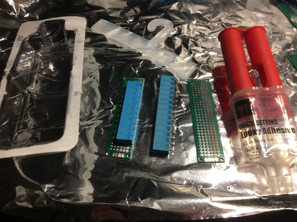
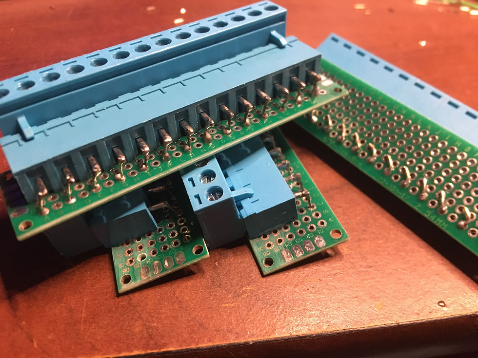
When the terminal blocks arrived, their pins were too large for the PCBs, as shown in the image below. To get around this, epoxy was used to join the side of the terminal blocks to their respective PCBs. The pins were then jumped to the PCB for easy connection.


The result of this is shown below.

On Saturday and Sunday, Ian and Daniel worked together to get the control module built up. The group knew that a lot of work was going to be involved but still underestimated just how much time would be required.
Ian took care of soldering while Daniel constructed the mounting surface. The first step was to solder the transistor array on PCB. To plan this out, a Google Sheet was used, as shown below. To make it easier to follow, the sheet was horizontally flipped just as the PCB was during soldering. It may look complicated and hard to read, but this sheet was invaluable during the soldering process, as it depicts exactly what gets connected and where.

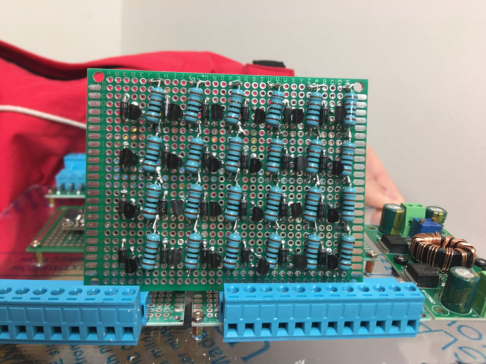
The front of the completed transistor array is shown below.

Before connecting everything to the MCU, some connections had to be made from the Pico PCB to the PCF PCB. The PCF Vin, Ground, SCL, and SCA connections were made, along with the LED anode connection.

Next, wires were run from the transistor array PCB to the Pico and PCF PCBs and soldered.


Comments